BIT Sindri: Two-day workshop on PCB design and fabrication begins
SUBHASH MISHRA Advertisement Dhanbad Nov 3: A two-day workshop on the PCB (Printed Circuit Board) design and fabrication began at BIT…

Faculty members and students in the workshop
SUBHASH MISHRA

Dhanbad Nov 3: A two-day workshop on the PCB (Printed Circuit Board) design and fabrication began at BIT Sindri on Friday.
An official of the institution said that the workshop is being organized by the Electronics and Communication Engineering Department (ECE) of BIT Sindri under the faculty development programme for students’ training.
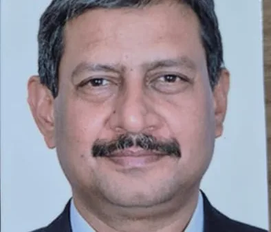
BIT Sindri director Prof. Pankaj Rai inaugurated the workshop along with ECE department head Prof. M.G. Tiwary. Dr Prashant Kumar Singh is the coordinator of the programme.
Gunjan Gandhi, a faculty member of the ECE department, Dr Amar Prakash Sinha, Dr Imteyaz Ahmad and more than 60 students from various academic backgrounds came together to delve into the intricacies of the PCB design and fabrication.
Duraswamy from ETS India Pvt. Ltd., Coimbatore, Tamil Nadu was present as the resource person in the workshop and he delivered insights and practical knowledge of the PCB design and fabrication and guided the students through the training modules.
A senior faculty member of the ECE department said that the workshop (training programme) offered a hands-on learning experience, allowing the students to gain in-depth knowledge about the essential tools and techniques required for PCB designing.
The participants were able to apply this knowledge practically and understand the nuances of designing printed circuit boards. Additionally, the program covered the fabrication process of a prototype of a PCB circuit, giving the students a comprehensive understanding of the entire PCB manufacturing cycle. This knowledge is invaluable, as it enables them to bring their innovative ideas to life and develop functional electronic devices.

“It not only provided students with practical skills but also fostered an environment of collaborative learning and innovation. The guidance of the program coordinators and the expertise of Duraswamy made this training a memorable and enriching experience for all participants, ensuring they are well-prepared for future endeavours in the field of PCB design and fabrication”, said an ECE department senior faculty member.